PCB Radiography Kindergarten.
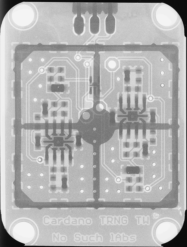
Below is the result of test-firing a newly-installed miniature PCB radiography system.
The victim is a standard FG TRNG Analogue Unit:
Click for full resolution (Warning: 14MB)
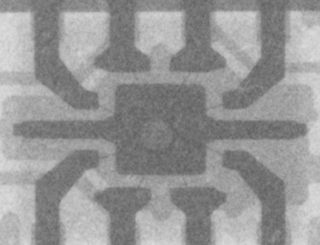
Detail of left op amp, with bonding whiskers visible:
The substrate, aluminum RF shield frame, SMT contacts, vias, and the two layers of the PCB are clearly distinguishable. Likewise resistors (nearly transparent) from capacitors (comparatively metal-heavy.)
Exposure: 100 sec. @ 32kV; 0.3mA @ 25cm. film: "Eco-30".
More interesting applications -- later.


